TM 11-5805-424-15/NAVELEX 0967-220-9012/TO 31W2-2G-41
C2
generated clock and the input timing
average dc voltage to the VCO. This
signal is achieved.
lower dc voltage causes the VCO to slow
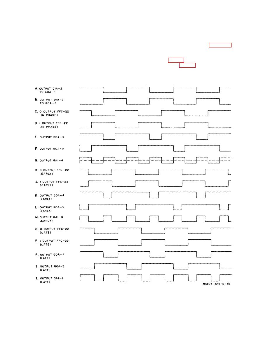
(b) Waveforms N and P, figure 5-8, indicate a
cause the generated bit-timing signal
generated bit-timing signal that is late with
(from FFC-22) to occur a little later, thus
respect to the bit-timing input (A and B,
moving toward the phase-lock condition of
90 out of phase with the input timing
4 (Q, fig. 5-8) being positive longer than it
signal. This operation continues until the
is negative, resulting in a higher average
phase-lock
condition
between
the
Figure 5-8. Phase-lock loop, timing waveforms.
5-20


