TM 11-5805-424-15/NAVELEX 0967-220-9010/TO 31W2-2G-41
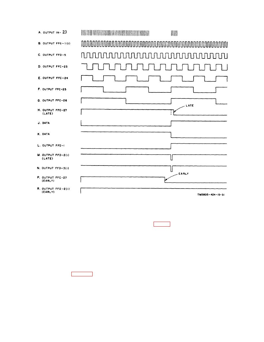
Figure 5-9. Receive timing add-subtract control logic waveforms.
5-22. Receive Data
8-5) is applied to the dual output polar drive
module, where either phase of the output from
bistable FFC-27 is strap-selectable. Risetime
a. Received fsk signals are coupled from the
and falltime shaper No. 1 provides a squared
BALANCED REC CARRIER INPUT terminals, through
bit-timing signal to drivers PDA-1 and PDA-2,
isolation transformer 1A1T3, to first input amplifier Q1.
which provide for two corrected bit-timing signal
INPUT switch 1A1S8 connects resistor A9R44 across
outputs to the external receiving equipment.
the primary of transformer 1A1T3 for operation with a
The bit-timing signal from the 0-output line of
600-ohm input line. First input amplifier Q1 provides a
bistable FFC-27 is also applied to the receive
reshaped signal to the delay equalizer (used only with
data output module, where the received data
MX-7379/G) and through resistor A9R3 to receive filter
signal is retimed for application to the external
FL1. The delay equalizer assembly provides equal
receiving equipment (para 5-22).
delay of the mark and space frequencies in the fsk input
Change 3
5-23


