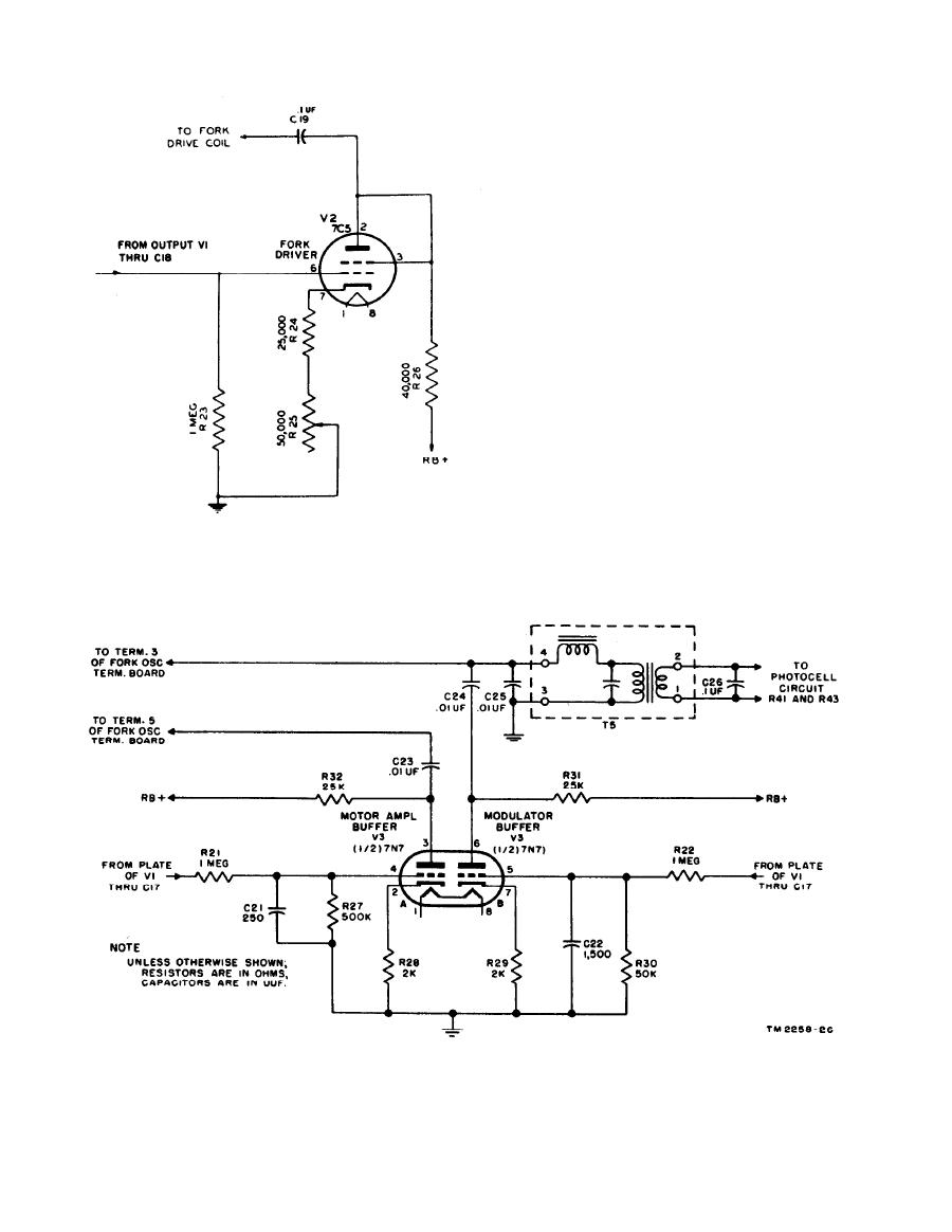
from the plate of V1 through coupling
capacitor C17 and limiting resistor R22.
Resistor R30 is the grid resistor, and the
grid is bypassed for high frequencies
by C22. Plate voltage is applied to
pin 6 from the regulated +250-volt
supply through plate load resistor R31.
Output from the plate is applied to the
circuit
modulator
photocell bridge
through blocking capacitor C24 and
output coupling transformer T5. The
output coupling circuit includes a low-
pass filter which eliminates harmonics of
the 1,800-cycle frequency and delivers
a sine-wave output to the modulator.
Components of this low-pass filter in-
clude hf shunt capacitors C25 and C26,
an audio choke, a capacitor, and an
output transformer. A connection to
section 2 of selector switch S1 short-
circuits the input of T5, removing 1,800-
cycle energy from the photocell circuit
when the selector switch is in the
Figure 36. Fork driver, unsealed fork oscillator unit.
S T A N D B Y , RECORD PHOTO, or
RECORD DIRECT position.
74


