TM 11-5805-424-15/NAVELEX 0967-220-9010/TO 31W2-2G-41
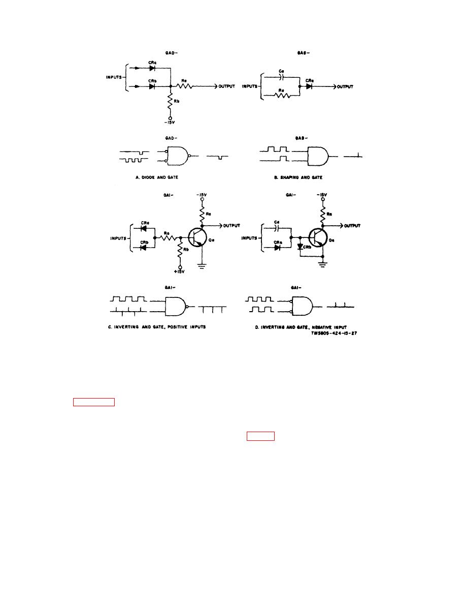
Figure 5-5. AND gate stages, schematic diagram and logic symbol.
regardless of the condition of the input
acts as the collector load resistor for
signal applied to capacitor Ca. Diode CRb
transistor Qa.
limits the forward bias of transistor Qa,
(b) The GAI-type AND gate shown in D,
and resistor Ra is the collector load
resistor.
volts) inputs to provide a high-level
output. A low-level applied to diode CRa
5-9. OR Gate Stages
is blocked (acting as an open circuit), so
input capacitor Ca controls circuit
operation, turning transistor Qa on when
the input is negative (providing a high-
a. General. Several types of OR gate stages are
level [ground] output), and turning it off
used in the equipment, all identical in operation. The
when the input is positive (providing a
only difference is in the input and output circuit
low-level [-15 volts] output). If the input to
configuration. In all cases, a high-level input on any
diode CRa is a high level, the high level is
passed by the diode to the base of
transistor Qa, maintaining it at cut off,
Change 3
5-8


