TM 11-5805-424-15/NAVELEX 0967-220-9010/TO 31W2-2G-41
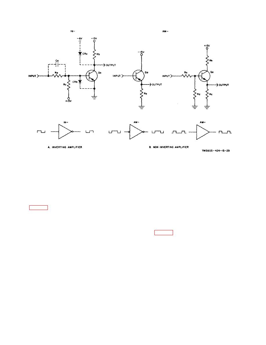
Figure 5-7. Amplifier stages, schematic diagram and logic symbol.
level output (developed across emitter resistor Rc).
operating bias for the stage; resistors Rb and Rc act to
Resistors Ra and Rd may be used to establish initial
limit the output voltage when transistor Qa conducts.
Section III. ANALOG CIRCUIT ANALYSIS
coupling resistor to emitter follower Q2. Resistor R4 is
5-11. Oscillator Circuits
the emitter self-biasing resistor for transistor Q2, used
as a buffer between the oscillator circuit and the output
load to prevent the undesired effects of loading.
a. The oscillator circuits used to develop mark and
space frequencies for the transmitted frequency-shift-
5-12. Oven Regulator
keying (fsk) data are identical Colpitts-type, crystal-
controlled oscillators, except for the crystal type and
values
of
frequency-determining
components
a. The oven regulator circuits maintain the oscillator
(capacitors C1 through C4 and inductor L1 and
oven temperature at a constant level to provide
capacitors C6 through C9 and inductor L2). These
maximum stability for the oscillator circuit. OVEN
component values are chosen according to the required
TEMP ADJUST resistor 1A1R1, in conjunction with
output frequencies. Only oscillator circuit Y1 (OSC-1) is
discussed in b below.
resistor 1A1R2, sets the initial bias for transistor Q1.
The resistance of thermistor A1RT1 varies inversely
b. Crystal Y1, capacitors C1 through C4, and inductor
with the external temperature; it provides greater current
L1 are the frequency-determining components.
through transistor Q1 when external temperature
Capacitor C5 provides the necessary feedback to
decreases
amplifier transistor Q1, to sustain oscillations. Resistor
R1 is the collector load resistor, R2 furnishes initial bias
for the oscillator stage, and R3 is the direct-current (dc)
Change 5
5-10


