TM 11-5805-424-15/NAVELEX 0967-220-9010/TO 31W2-2G-41
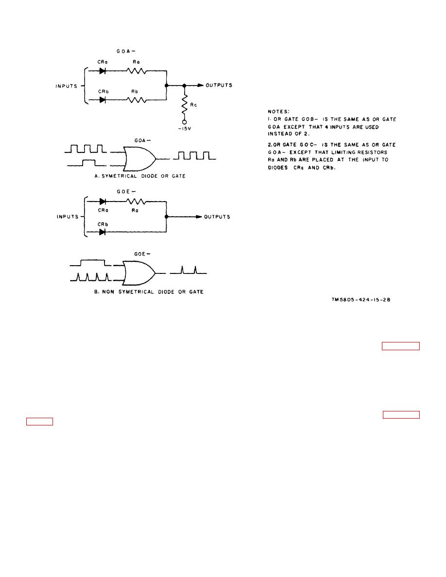
Figure 5-6. OR gate stages, schematic diagram and logic symbol.
put on any input line provides a high level at the output.
b. Circuit Analysis.
b. Circuit Analysis. The input diodes pass only the
(1) In the amplifier circuit shown in A, figure 5-7,
high-level signals, and the input resistors act as series
resistor Ra is a limiting resistor and may be
limiters to protect subsequent circuitry. The enabled
bridged by speedup capacitor Ca. Resistor Rc
output of each gate is a high level (ground). The
provides initial bias for the stage, and resistor Rb
inhibited output of OR gates GOA-, GOB-, and GOC- is
is the collector load resistor. Optional diode
a low-level -15 volts; the inhibited output of OR gate
CRb acts to limit the forward bias of transistor
GOE is absence of output (open circuit).
Qa. Optional diode CRb acts to clamp the cutoff
output to -6 volts.
5-10. Amplifier Stages
(2) In the amplifier circuits shown in B, figure 5-7,
PNP transistor Qa (left side) uses resistor Ra as
the emitter-load resistor to provide a low-level
output. NFN transistor Qa (right side) is used to
a. General. Two types of digital amplifier circuits
provide a low-level output (developed across
are used in the equipment: the inverting type IN-, which
emitter resistor Rc). An NPN transistor is used
provides output inversion of the input signal, and the
in some cases to provide a high
noninverting or emitter follower type AM-.
Change 5
5-9


