modulator circuit as explained in para-
the LINE binding posts through section
graph 74. Resistor R50 serves as the
1 of the selector switch, or to the high
grid resistor, across which the modulated
end of R60 from the LINE JACK
1,800-cycle signal is developed and ap-
through section 3 of the switch, depend-
ing on the input connections in use (par.
plied to the grid. Cathode bias is
developed across R51 and filtered by
the same for receiving as for transmitting.
C32. The screen is fed through R52
and bypassed directly to the cathode by
C33. Resistor R53 is the plate load
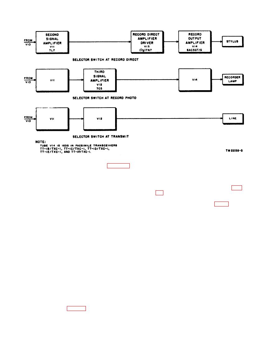
second signal amplifier is a pentode voltage am-
resistor. An amplified modulated 1,800-
plifier tube 7L7, biased for Class A operation
cycle signal is developed across this
and used without circuit changes for both
resistor and applied to the grid of tube
transmitting and receiving. The input is from
V11 through output coupling capacitor
stage V10 and its output feeds V12 through the
C35. Resistor R54 and capacitor C34
transmitting portion of the dual GAIN control
form a resistance-capacitance decoupling
(R59) and also both triode sections of the signal
meter amplifier (V13). The input signal (the
network between the stage and the source
of regulated B+ plate and screen volt-
modulated 1,800 cycles from V10) is applied
ages.
through C35 and across grid resistor R55 to the
(2) Receiving. With the selector switch in the
control grid of V11. Capacitor C35 is a low value
recording positions, the bridge modulator
capacitor used to attenuate unwanted low-fre-
is inactive. The control grid of V10 is
quency signals from the previous stage. In Fac-
simile Transceivers TT-1/TXC-1 through TT-
connected through R50 as a series resistor
and S1 is connected to the arm on control
1C/TXC-1, C35 is 100 micromicrofarad (f).
R60, that half of the dual GAIN control
Cathode bias for Class A operation is developed
which serves as an input gain control
by current flow through cathode resistor R56,
which is bypassed at audio frequencies by C36.
across the secondary of input trans-
former T7 (figs. 163 through 169). In-
In Facsimile Transceiver TT-1D/TXC-1, cou-
put to the transceiver is either through
pling capacitor C35 is increased to 5,100 f (the
this line-matching transformer (T7) from
same as C38) and grid resistor R55 to 470,000
88


