TM 11-5820-803-12
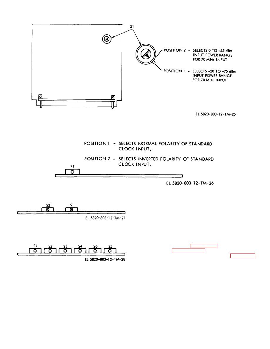
Figure 2-21. 70 MHz input signal range selection switch S1 (viewed from component side of input filter card, SM-D-
7S1133: A2A1A1A22).
Figure 2-22. Standard clock input inverter switch S1 (viewed from top of input interface card, SM-D-742037, A2AA2A4).
direct
support
maintenance
personnel.
If the PSK modem installation requires interface with a
remote digital user over either a shielded cable or a line-
of-sight (LOS) microwave link, the LOS/cable receiver
Figure 2-23. Line driver polarity inverter switches S1 and
and decoder card must be configured to suit the system
S2 (viewed from top of line driver card, SM-D-742053,
requirements. This is accomplished by setting the
A2A2A1A21, A1A2A1A22, A1A2A1A23).
switches on the LOS/cable receiver and decoder card,
shown functionally in figure 2-27, according to the
instructions in paragraph 2-20f. Then the card must be
aligned per the following procedure (refer to figure 2-26
for location of controls and test points):
NOTE
Figure 2-24. External coder interface clock inverter
It is recommended that any spare
switches S1 through S6 (viewed from top of coder
LOS/ cable receiver and decoder
interface card, SM-A-74049, A2A2A2A5).
cards (SM-D742089) provided on the
site also be placed in the modem and
2-21. Circuit Lineup
aliened prior to placing the modem in
NOTE
service.
The following installation procedures
a. The initial adjustments are made at a data rte of
must be made with the assistance of
5.0000 Mb/s regardless of the normal system
2-24


